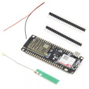
ILYGO® TTGO T-Call V1.3 ESP32 Wireless Module GPRS Antenna SIM Card SIM800L Board: Difference between revisions

From B-Wiki
Jump to navigation Jump to search
(Created page with "{| class="wikitable" style="float:right; margin-left: 10px;" | {{FULLPAGENAME}} | {{#qrlite:{{fullurl:{{FULLPAGENAME}}}}|format=svg|size=2|ecc=1|margin=0}} |- | colspan="2"|...")
 
mNo edit summary
 
(4 intermediate revisions by the same user not shown)
Line 8: Line 8:
== Features ==
== Features ==


PCF8591 is a single-supply, low-power 8 COMS-type A / D, D / A converter chip, it has a 4-channel analog input channels, all the way to the analog output channels and an I2C bus interface. The device I2C slave address lower three chips A0, A1 and A2, three address pins decision so without adding any hardware with an I2C bus can connect up to eight devices of the same type. The device has a multi-channel analog input, on-chip track-and-hold, 8 A / D conversion and eight D / A conversion functions. A / D and D / A conversion rate determined by a maximum transfer rate of the I2C bus.


Characteristics:
[[File:Module ILYGO® TTGO T-Call V1.3 ESP32 Wireless Module GPRS Antenna SIM Card SIM800L Board.jpg|thumb|Module ILYGO® TTGO T-Call V1.3 ESP32 Wireless Module GPRS Antenna SIM Card SIM800L Board]]


# Single power supply;
More Information: https://github.com/Xinyuan-LilyGO/TTGO-T-Call
# The normal operating supply voltage range of 2.5V ~ 6V;
# Completed through the I2C bus data input / output;
# Device address is determined by three address pins;
# The sampling frequency is decided by the I2C bus transfer rate;
# The 4 Road analog inputs programmable as single-ended or differential inputs;
# Can be configured to convert the channel number is automatically increased functionality;
# The analog voltage range of VSS ~ VDD;
# On-chip track-and-hold function;
# 8-bit successive approximation A / D conversion;
# Multiplication with one analog output D / A converter.


Module Description:
Package includes:
* Module chip with PCF8591T, SMD package
* Support 4 channel analog voltage the acquisition signal input (voltage input range of 0 - 5V)
* Module with power indicator 1 (D1)
* A module with DA output indicator (D2), when the DA output voltage reaches a certain value, the indicator light, the higher the voltage value, the brighter lights
* The module integrates a Road 0 - 5V voltage input acquisition (through the blue and white potentiometer to adjust the input voltage)
* The module Integrated Road the photoresistor (Model: 5537), ambient light intensity by AD collection
* Module integrated way thermistor (Model: MF58) ambient temperature by AD collection
* PCB size: 48mm * 25mm * 1.6mm
* Quality panel corners arc design will not scratch your hand. With a positioning hole aperture 3.1mm, easy to use 3mm Tongzhu fixed


Wiring instructions:
# 1 x T-Call V1.3
# 1 x Power cord
# 2 x Pin header
# 1 x GPRS antenna (9cm)


Left 4 pin:
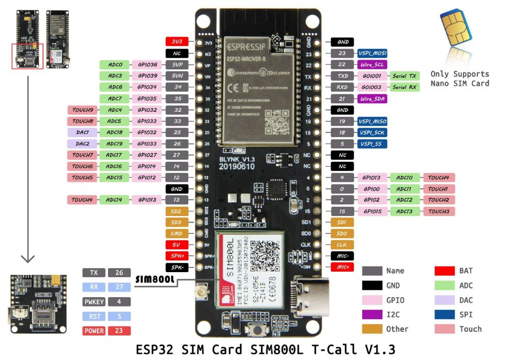
=== Schematic ===
[[File:Schematic ILYGO® TTGO T-Call V1.3 ESP32 Wireless Module GPRS Antenna SIM Card SIM800L Board.jpg|1000px]]


* SDA IIC data interface connected microcontroller IO ports (P2.0)
Hardware Specifications
* SCL IIC clock interface connected microcontroller IO port (P2.1)
* The cathode interface external VCC power 3.3/5V positive power supply
* GND Negative interface external 3.3/5V negative supply


Right 8 pin :
* Chipset ESPRESSIF-ESP32 240MHz Xtensa® dual-core 32-bit LX6 microprocessor
* AOUT module DA output port
* FLASH QSPI flash 4MB / PSRAM  8MB
* AIN3 analog input signal interface
* SRAM 520 kB SRAM
* AIN2 analog input signal interface
* Button Reset
* AIN1 analog input signal interface
* USB to TTL CP2104
* AIN0 analog input signal interface 0
* Modular interface UART, SPI, SDIO, I2C, LED PWM, TV PWM, I2S, IRGPIO, capacitor touch sensor, ADC, DACLNA  pre-amplifier
* The INPUT3 analog input signal interface 3
* On-board clock 40MHz crystal oscillator
* INPUT2 thermistor signal input port is connected to
* Working voltage 2.7V-3.6V
* The INPUT1 has photoresistor signal input port connected to theINPUT0 is connected to the signal input port of the potentiometer
* Working current About 70mA
* Sleep current About 300uA
* SIM card Only supports Nano SIM card
* Working temperature range -40℃ ~ +85℃
* Size&Weight 78.83mm*28.92mm*8.06mm(11.77g)
* Power Supply Specifications
* Power Supply USB 5V/1A
* Charging current 500mA
* Battery 3.7V lithium battery
* JST Connector 2Pin 1.25mm
* USB Type-C
* Wi-Fi
* Standard FCC/CE-RED/IC/TELEC/KCC/SRRC/NCC
* Protocol 802.11 b/g/n(802.11n, speed up to150Mbps)A-MPDU and A-MSDU polymerization, support 0.4μS Protection interval
* Frequency range 2.4GHz~2.5GHz(2400M~2483.5M)
* Transmit Power 22dBm
* Communication distance 300mbluetooth
* Protocol meet bluetooth v4.2BR/EDR and BLE standard
* Radio frequency with -97dBm sensitivity NZIF receiver Class-1,Class-2&Class-3 emitter AFH
* Audio frequency CVSD&SBC audio frequency


[[File:PCF8591 AD - DA Converter Module Analog to digital conversion module.jpg|thumb|PCF8591 AD - DA Converter Module Analog to digital conversion module]]


Software specification
* Wi-Fi Mode Station/SoftAP/SoftAP+Station/P2P
* Security mechanism WPA/WPA2/WPA2-Enterprise/WPS
* Encryption Type AES/RSA/ECC/SHA
* Firmware upgrade UART download/OTA(Through network/host to download and write firmware)
* Software Development Support cloud server development /SDK for user firmware development
* Networking protocol IPv4, IPv6, SSL, TCP/UDP/HTTP/FTP/MQTT
* User Configuration AT + Instruction set, cloud server, android/iOSapp
* OS FreeRTOS


The PCF8591 module consists of a master control chip PCF8591, some resistors and capacitors .It can data acquisition device and has four analog inputs, one analog output and a serial I2C-bus interface. Three address pins A0, A1 and A2 are used for programming the hardware address, allowing the use of up to eight devices connected to the I2C-bus without additional hardware. Address, control and data to and from the device are transferred serially via the two-line bidirectional I2C-bus.
Software for the gateway: [https://github.com/tinel-c/PlatformIO_Arduino_SIM800_ESP32]
The schematic diagram of the module is as follows:
[[File:PCF8591 AD module schematic.png]]
 
<font color="red">
Note:<br>
From the schematic diagram, a potentiometer is connected to AIN0. You can connect the P3 by the jumper cap, which is to wire the two pins next to the pot, so the pot can be used as the input of AIN0.
</font>
 
=='''PCF8591'''==
The PCF8591 is a single-chip, single-supply low power 8-bit CMOS data acquisition device with four analog inputs, one analog output and a serial I2C-bus interface. Three address pins A0, A1 and A2 are used for programming the hardware address, allowing the use of up to eight devices connected to the I2C-bus without additional hardware. Address, control and data to and from the device are transferred serially via the two-line bidirectional I2C-bus.
The functions of the device include analog input multiplexing, on-chip track and hold function, 8-bit analog-to-digital conversion and an 8-bit digital-to-analog conversion. The maximum conversion rate is given by the maximum speed of the I2C-bus.
===Block Diagram===
[[File:PCF8591 AD block diagram.png]]
 
===Pin Function===
[[File:PCF8591 AD pin function package.png]]
[[File:PCF8591 AD pin function.png]]
 
=='''Features'''==
*Support acquisition of external 4-line voltage inputs (ranging 0-5v), with a single power supply
*Standard double-sided printed circuit board, 1.16mm thick, with an elegant layout, 3-mm holes at each corner for easy fixing
*Use an 8-bit successive approximation A/D converter
*Input/output by an I2C bus
*Working voltage: 2.5-6V DC; PCB size: 2.4 x 2.8 cm
*Single supply, low standby current
*Address by 3 hardware address pins
=='''Resource'''==
[https://www.nxp.com/docs/en/data-sheet/PCF8591.pdf Data sheet]
 
[https://www.sunfounder.com/learn/Sensor-Kit-v2-0-for-Arduino/lesson-33-analog-digital-converter-sensor-kit-v2-0-for-arduino.html Test Experiment for Arduino]
 
[https://www.sunfounder.com/learn/sensor-kit-v2-0-for-raspberry-pi-b-plus/lesson-13-pcf8591-sensor-kit-v2-0-for-b-plus.html Test Experiment for Raspberry Pi]


[[Category:Data conversion modules]]
[[Category:Data conversion modules]]

Latest revision as of 11:49, 7 May 2023

ILYGO® TTGO T-Call V1.3 ESP32 Wireless Module GPRS Antenna SIM Card SIM800L Board

https://bogza.ro/index.php/ILYGO%C2%AE_TTGO_T-Call_V1.3_ESP32_Wireless_Module_GPRS_Antenna_SIM_Card_SIM800L_Board

Features

Module ILYGO® TTGO T-Call V1.3 ESP32 Wireless Module GPRS Antenna SIM Card SIM800L Board

More Information: https://github.com/Xinyuan-LilyGO/TTGO-T-Call

Package includes:

  1. 1 x T-Call V1.3
  2. 1 x Power cord
  3. 2 x Pin header
  4. 1 x GPRS antenna (9cm)

Schematic

Hardware Specifications

  • Chipset ESPRESSIF-ESP32 240MHz Xtensa® dual-core 32-bit LX6 microprocessor
  • FLASH QSPI flash 4MB / PSRAM 8MB
  • SRAM 520 kB SRAM
  • Button Reset
  • USB to TTL CP2104
  • Modular interface UART, SPI, SDIO, I2C, LED PWM, TV PWM, I2S, IRGPIO, capacitor touch sensor, ADC, DACLNA pre-amplifier
  • On-board clock 40MHz crystal oscillator
  • Working voltage 2.7V-3.6V
  • Working current About 70mA
  • Sleep current About 300uA
  • SIM card Only supports Nano SIM card
  • Working temperature range -40℃ ~ +85℃
  • Size&Weight 78.83mm*28.92mm*8.06mm(11.77g)
  • Power Supply Specifications
  • Power Supply USB 5V/1A
  • Charging current 500mA
  • Battery 3.7V lithium battery
  • JST Connector 2Pin 1.25mm
  • USB Type-C
  • Wi-Fi
  • Standard FCC/CE-RED/IC/TELEC/KCC/SRRC/NCC
  • Protocol 802.11 b/g/n(802.11n, speed up to150Mbps)A-MPDU and A-MSDU polymerization, support 0.4μS Protection interval
  • Frequency range 2.4GHz~2.5GHz(2400M~2483.5M)
  • Transmit Power 22dBm
  • Communication distance 300mbluetooth
  • Protocol meet bluetooth v4.2BR/EDR and BLE standard
  • Radio frequency with -97dBm sensitivity NZIF receiver Class-1,Class-2&Class-3 emitter AFH
  • Audio frequency CVSD&SBC audio frequency


Software specification

  • Wi-Fi Mode Station/SoftAP/SoftAP+Station/P2P
  • Security mechanism WPA/WPA2/WPA2-Enterprise/WPS
  • Encryption Type AES/RSA/ECC/SHA
  • Firmware upgrade UART download/OTA(Through network/host to download and write firmware)
  • Software Development Support cloud server development /SDK for user firmware development
  • Networking protocol IPv4, IPv6, SSL, TCP/UDP/HTTP/FTP/MQTT
  • User Configuration AT + Instruction set, cloud server, android/iOSapp
  • OS FreeRTOS

Software for the gateway: [1]