PCF8591 AD / DA Converter Module Analog to digital conversion module: Difference between revisions
| Line 39: | Line 39: | ||
*Address by 3 hardware address pins | *Address by 3 hardware address pins | ||
=='''Resource'''== | =='''Resource'''== | ||
[https://www.nxp.com/docs/en/data-sheet/PCF8591.pdf] | [https://www.nxp.com/docs/en/data-sheet/PCF8591.pdf Data sheet] | ||
[https://www.sunfounder.com/learn/Sensor-Kit-v2-0-for-Arduino/lesson-33-analog-digital-converter-sensor-kit-v2-0-for-arduino.html Test Experiment for Arduino][[File:LINK.jpg]]<br> | [https://www.sunfounder.com/learn/Sensor-Kit-v2-0-for-Arduino/lesson-33-analog-digital-converter-sensor-kit-v2-0-for-arduino.html Test Experiment for Arduino][[File:LINK.jpg]]<br> | ||
[https://www.sunfounder.com/learn/sensor-kit-v2-0-for-raspberry-pi-b-plus/lesson-13-pcf8591-sensor-kit-v2-0-for-b-plus.html Test Experiment for Raspberry Pi][[File:LINK.jpg]] | [https://www.sunfounder.com/learn/sensor-kit-v2-0-for-raspberry-pi-b-plus/lesson-13-pcf8591-sensor-kit-v2-0-for-b-plus.html Test Experiment for Raspberry Pi][[File:LINK.jpg]] | ||
Revision as of 08:59, 16 June 2019
| PCF8591 AD / DA Converter Module Analog to digital conversion module |
|
| https://bogza.ro/index.php/PCF8591_AD_/_DA_Converter_Module_Analog_to_digital_conversion_module | |
Features
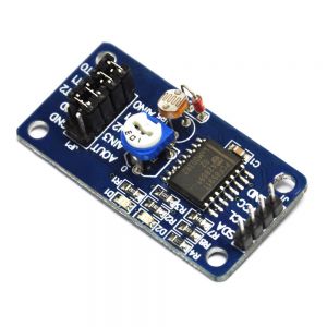
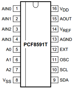
The PCF8591 module consists of a master control chip PCF8591, some resistors and capacitors .It can data acquisition device and has four analog inputs, one analog output and a serial I2C-bus interface. Three address pins A0, A1 and A2 are used for programming the hardware address, allowing the use of up to eight devices connected to the I2C-bus without additional hardware. Address, control and data to and from the device are transferred serially via the two-line bidirectional I2C-bus.
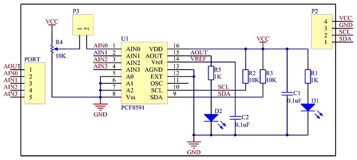
The schematic diagram of the module is as follows:
Note:
From the schematic diagram, a potentiometer is connected to AIN0. You can connect the P3 by the jumper cap, which is to wire the two pins next to the pot, so the pot can be used as the input of AIN0.
PCF8591
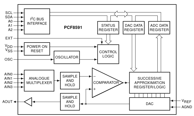
The PCF8591 is a single-chip, single-supply low power 8-bit CMOS data acquisition device with four analog inputs, one analog output and a serial I2C-bus interface. Three address pins A0, A1 and A2 are used for programming the hardware address, allowing the use of up to eight devices connected to the I2C-bus without additional hardware. Address, control and data to and from the device are transferred serially via the two-line bidirectional I2C-bus. The functions of the device include analog input multiplexing, on-chip track and hold function, 8-bit analog-to-digital conversion and an 8-bit digital-to-analog conversion. The maximum conversion rate is given by the maximum speed of the I2C-bus.
Block Diagram
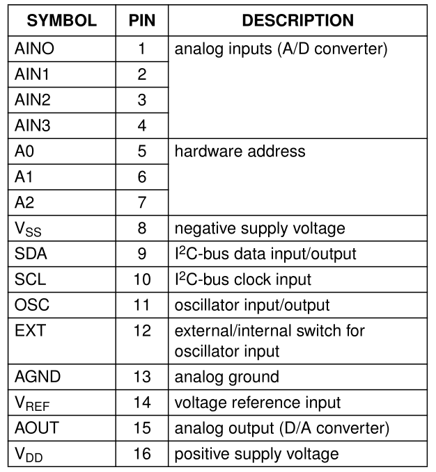
Pin Function
Features
- Support acquisition of external 4-line voltage inputs (ranging 0-5v), with a single power supply
- Standard double-sided printed circuit board, 1.16mm thick, with an elegant layout, 3-mm holes at each corner for easy fixing
- Use an 8-bit successive approximation A/D converter
- Input/output by an I2C bus
- Working voltage: 2.5-6V DC; PCB size: 2.4 x 2.8 cm
- Single supply, low standby current
- Address by 3 hardware address pins
Resource
Data sheet
Test Experiment for ArduinoFile:LINK.jpg
Test Experiment for Raspberry PiFile:LINK.jpg
