Smart presence sensor T19SMWV01: Difference between revisions
Jump to navigation
Jump to search
| Line 26: | Line 26: | ||
=== IO config sheet === | === IO config sheet === | ||
[[File:Arduino-Nano-Pinout.jpg|frame|center|Arduino Nano Pinout]] | [[File:Arduino-Nano-Pinout.jpg|frame|center|Arduino Nano Pinout]] | ||
{| class="wikitable" | |||
! Mapping | |||
! Arduino PIN | |||
! Pin Function | |||
! Serial Pin | |||
! PORT | |||
! Board pin name | |||
! rowspan="16" | | |||
! Board pin name | |||
! PORT | |||
! ADC | |||
! Serial Pin | |||
! Arduino PIN | |||
! Mapping | |||
|- | |||
| | |||
| 1 | |||
| | |||
| TXD | |||
| PD1 | |||
| TX1 | |||
| VIN | |||
| | |||
| | |||
| | |||
| | |||
| | |||
|- | |||
| | |||
| 0 | |||
| | |||
| RXD | |||
| PD0 | |||
| RX0 | |||
| GND | |||
| | |||
| | |||
| | |||
| | |||
| | |||
|- | |||
| | |||
| | |||
| | |||
| | |||
| PC6 | |||
| RST | |||
| RST | |||
| PC6 | |||
| | |||
| | |||
| | |||
| | |||
|- | |||
| | |||
| | |||
| | |||
| | |||
| | |||
| GND | |||
| 5V | |||
| | |||
| | |||
| | |||
| | |||
| | |||
|- | |||
| | |||
| 2 | |||
| INT0 | |||
| | |||
| PD2 | |||
| D2 | |||
| A7 | |||
| | |||
| ADC7 | |||
| | |||
| A7 | |||
| | |||
|- | |||
| | |||
| 3 | |||
| OC2B / INT1 | |||
| | |||
| PD3 | |||
| D3 | |||
| A6 | |||
| | |||
| ADC6 | |||
| | |||
| A6 | |||
| | |||
|- | |||
| | |||
| 4 | |||
| XCK / T0 | |||
| | |||
| PD4 | |||
| D4 | |||
| A5 | |||
| PC5 | |||
| ADC5 | |||
| SCL | |||
| 19 A5 | |||
| | |||
|- | |||
| | |||
| 5 | |||
| OC0B / T1 | |||
| | |||
| PD5 | |||
| D5 | |||
| A4 | |||
| PC4 | |||
| ADC4 | |||
| SDA | |||
| 18 A4 | |||
| | |||
|- | |||
| | |||
| 6 | |||
| OC0A / AIN0 | |||
| | |||
| PD6 | |||
| D6 | |||
| A3 | |||
| PC3 | |||
| ADC3 | |||
| | |||
| 17 A3 | |||
| | |||
|- | |||
| | |||
| 7 | |||
| AIN1 | |||
| | |||
| PD7 | |||
| D7 | |||
| A2 | |||
| PC2 | |||
| ADC2 | |||
| | |||
| 16 A2 | |||
| | |||
|- | |||
| | |||
| 8 | |||
| ICP1 / CLKO | |||
| | |||
| PB0 | |||
| D8 | |||
| A1 | |||
| PC1 | |||
| ADC1 | |||
| | |||
| 15 A1 | |||
| | |||
|- | |||
| | |||
| 9 | |||
| OC1A | |||
| | |||
| PB1 | |||
| D9 | |||
| A0 | |||
| PC0 | |||
| ADC0 | |||
| | |||
| 14 A0 | |||
| | |||
|- | |||
| | |||
| 10 | |||
| OC1B | |||
| ~SS | |||
| PB2 | |||
| D10 | |||
| REF | |||
| | |||
| AREF | |||
| | |||
| | |||
| | |||
|- | |||
| | |||
| 11 | |||
| OC2 | |||
| MOSI | |||
| PB3 | |||
| D11 | |||
| 3V3 | |||
| | |||
| | |||
| | |||
| | |||
| | |||
|- | |||
| | |||
| 12 | |||
| | |||
| MISO | |||
| PB4 | |||
| D12 | |||
| D13 | |||
| PB5 | |||
| | |||
| SCK | |||
| 13 | |||
| | |||
|} | |||
Revision as of 07:26, 7 April 2019
| Smart presence sensor T19SMWV01 |
|
| https://bogza.ro/index.php/Smart_presence_sensor_T19SMWV01 | |

Description
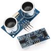
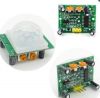
Sensor has been designed to have 3 motion / distance sensors that couple together to give an accurate reading of the presence inside one room.
Specification
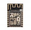
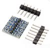
Modules used
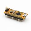
IO config sheet

| Mapping | Arduino PIN | Pin Function | Serial Pin | PORT | Board pin name | Board pin name | PORT | ADC | Serial Pin | Arduino PIN | Mapping | |
|---|---|---|---|---|---|---|---|---|---|---|---|---|
| 1 | TXD | PD1 | TX1 | VIN | ||||||||
| 0 | RXD | PD0 | RX0 | GND | ||||||||
| PC6 | RST | RST | PC6 | |||||||||
| GND | 5V | |||||||||||
| 2 | INT0 | PD2 | D2 | A7 | ADC7 | A7 | ||||||
| 3 | OC2B / INT1 | PD3 | D3 | A6 | ADC6 | A6 | ||||||
| 4 | XCK / T0 | PD4 | D4 | A5 | PC5 | ADC5 | SCL | 19 A5 | ||||
| 5 | OC0B / T1 | PD5 | D5 | A4 | PC4 | ADC4 | SDA | 18 A4 | ||||
| 6 | OC0A / AIN0 | PD6 | D6 | A3 | PC3 | ADC3 | 17 A3 | |||||
| 7 | AIN1 | PD7 | D7 | A2 | PC2 | ADC2 | 16 A2 | |||||
| 8 | ICP1 / CLKO | PB0 | D8 | A1 | PC1 | ADC1 | 15 A1 | |||||
| 9 | OC1A | PB1 | D9 | A0 | PC0 | ADC0 | 14 A0 | |||||
| 10 | OC1B | ~SS | PB2 | D10 | REF | AREF | ||||||
| 11 | OC2 | MOSI | PB3 | D11 | 3V3 | |||||||
| 12 | MISO | PB4 | D12 | D13 | PB5 | SCK | 13 |